In short
Kepler Computing has emerged from stealth with $468 million in funding and a claim that its new memory architecture can help ease AI chip shortages. The startup says its 3D-stacked HBM and ferroelectric SRAM approaches could scale in existing fabs without relying on EUV lithography.
- Kepler Computing has emerged from stealth after seven years with a new memory architecture and $468 million in funding.
- The startup says its 3D-stacked HBM and ferroelectric SRAM could reduce dependence on EUV-heavy chip production.
- GlobalFoundries, Intel Capital, AMD Ventures, Bill Gates and the US Commerce Department are among its backers.
- Kepler plans to ship HBM samples this year, ramp in Singapore next year and begin US production in 2028.
- The biggest challenge ahead is scaling from about 2,000 wafers to reliable high-volume manufacturing.
Kepler Computing, a San Jose startup that has worked in stealth since 2018, has emerged with a large funding war chest and a bold claim: it can ease the AI memory bottleneck by rethinking how high-bandwidth memory and SRAM are built. The company says its new architecture could improve supply without waiting for expensive new fabs to come online, a promise that matters as data-center demand keeps straining the chip industry.
The startup says its approach could help relieve a global shortage of memory chips at a moment when AI systems are pushing hardware supply chains to their limits. If Kepler can manufacture at scale, its technology could become one of the more consequential attempts yet to reshape the economics of advanced memory production.
Why AI has turned memory into a choke point
AI has changed the memory market faster than many chipmakers expected. Training and running large models requires enormous data movement, and that has elevated high-bandwidth memory, or HBM, from a niche component into one of the most sought-after parts in the semiconductor stack.
HBM matters because it sits close to compute chips and moves large amounts of data quickly, reducing bottlenecks in systems built around GPUs, CPUs and other accelerators. As model sizes and inference workloads have expanded, the need for fast, efficient memory has grown alongside them.
That shift has exposed a hard reality: memory production cannot be expanded overnight. Building new fabrication plants is expensive, slow and technically demanding. Even when demand is obvious, supply can lag for years.
Kepler’s thesis is that the industry does not necessarily need to wait for a wave of new factories. Instead, it can wring more capacity out of existing manufacturing infrastructure by changing the memory architecture itself.
What Kepler says it has built
Kepler says it has developed a new method for producing HBM using 3D stacking and a proprietary material system that increases density without depending on extreme ultraviolet lithography, better known as EUV. That is a notable claim because EUV is one of the most expensive and infrastructure-heavy parts of modern chipmaking.
In conventional semiconductor manufacturing, EUV is used to shrink transistors and pack more capability into a smaller physical space. Kepler is arguing for a different route: rather than relying on ever more advanced lithography, it says it can achieve similar density gains through stack design and materials innovation.
The company also says it has applied a related idea to SRAM, the fast cache memory used inside chips to reduce latency. Kepler claims its SRAM work can approach the density of 2-nanometer or 3-nanometer chips without requiring a comparable investment in EUV-heavy production lines.
How does Kepler say its memory architecture works?
Kepler says the answer is a mix of 3D packaging, lower-voltage materials and existing semiconductor tools. For HBM, the company says it has developed a manufacturing technique that fits more memory into a fixed footprint, allowing the compute core to sit closer to the memory and move data with less energy.
For SRAM, the startup says it is using ferroelectric materials and a new composite material to improve how data is read and written at lower voltages. In theory, that reduces power use while preserving the speed advantages that make SRAM attractive in high-performance chips.
“Once we found a way to solve the physics problem, we came up with a material innovation that helps with the amount of memory you can have between chips,” said Sasi Manipatruni, a Kepler cofounder and chief technology officer.
The company says the work required substantial trial and error. Manipatruni said the team iterated through 35 composite formulations before finding a class of materials they believed could make the process easier and cheaper.
A table of the key facts
| Category | Kepler’s claim | Why it matters |
|---|---|---|
| Company | Kepler Computing | Stealth startup focused on next-generation memory |
| Founded | 2018 | Has spent more than seven years developing the technology |
| Total funding | $468 million | Backed by major investors and strategic chip players |
| Government support | Up to $245 million from the US Commerce Department | Signals policy interest in domestic AI memory production |
| Core technology | 3D-stacked HBM and ferroelectric SRAM | Designed to increase density without EUV dependence |
| Near-term timeline | First HBM samples later this year | Important proof point before commercial scaling |
| Production plan | Singapore next, US production in 2028 | Shows a phased manufacturing ramp |
Who is backing the startup?
Kepler has attracted an unusually high-profile set of backers for a company still working toward mass production. Its investors include GlobalFoundries, Intel Capital, AMD Ventures, the British fund Baillie Gifford and Bill Gates through his Gates Frontier vehicle.
The company also received a major commitment from the US government. In July, the Department of Commerce said it would provide up to $245 million to support development of what it described as a new class of high-performance AI memory technology built around 3D and ferroelectric approaches.
The combination of strategic investors and public funding suggests Kepler is being viewed not just as a startup bet, but as part of a larger push to strengthen domestic semiconductor capacity in a market increasingly shaped by AI demand.
Intel Capital’s managing director, Srini Ananth, said the firm never assumed Kepler would replace traditional memory products outright, but saw room for the market to determine where the technology fits as demand grows for both SRAM and HBM.
Why GlobalFoundries matters to Kepler’s plan
GlobalFoundries is central to Kepler’s near-term manufacturing strategy. The foundry is both an investor and a production partner, and Kepler says much of its testing has been done in Singapore, where GlobalFoundries has a facility.
Over the past two years, Kepler has built what it calls mini fabs, working alongside GlobalFoundries’ 28-nanometer processes. It has also run tests in GlobalFoundries’ Burlington, Vermont, facilities.
For Kepler, that relationship is part of the pitch. The company argues that its approach can be inserted into existing manufacturing ecosystems rather than requiring an entirely new generation of plants and tools.
“It’s a new materials system, with multigenerational scaling potential, without having to build entirely new systems in the fab or invest in very expensive lithography equipment,” said Ed Kaste, senior vice president of GlobalFoundries’ CMOS business.
That endorsement is meaningful because it frames Kepler’s technology as a practical industrial upgrade rather than a theoretical lab project.
How much money and time could the industry save?
Kepler’s core economic argument is that retooling an existing fab may be much cheaper than building a new one. The startup says its methods can avoid the need for the tens of billions of dollars typically required to build and equip a new advanced semiconductor plant.
New fabs often cost between $20 billion and $40 billion, and that price tag can rise further when including specialized equipment and integration costs. Kepler’s bet is that even if its materials and process changes require additional investment, the total should remain far below the cost of starting from scratch.
The company also says one of its early manufacturing exercises showed how fast a fab could be reconfigured. Kepler claims it converted a fabrication line into a next-generation setup in eight months, a process it says would usually take about 24 months.
If those timelines prove repeatable, the implications would be significant. A faster conversion cycle could make memory manufacturing more responsive to market swings and help fabs adapt to fast-changing AI demand.
What is the technical appeal of 3D stacking?
3D stacking is attractive because it packs more functionality into the same footprint. In HBM, that means more memory can be placed close to compute, shortening the data path and reducing both latency and energy use.
Kepler says its eventual goal is to move data in HBM with energy efficiency closer to that of SRAM while preserving HBM’s large capacity. That combination would be highly valuable for AI systems, where both speed and energy efficiency matter.
Researchers and chipmakers have long looked for ways to improve memory density without continually shrinking transistors. Kepler is trying to exploit that pressure point by changing the architecture instead of simply making the same device smaller.
What are the risks?
Kepler still has to prove that its lab results can survive real-world manufacturing. Semiconductor history is full of ideas that looked promising in controlled settings but ran into problems when scaled to thousands or millions of devices.
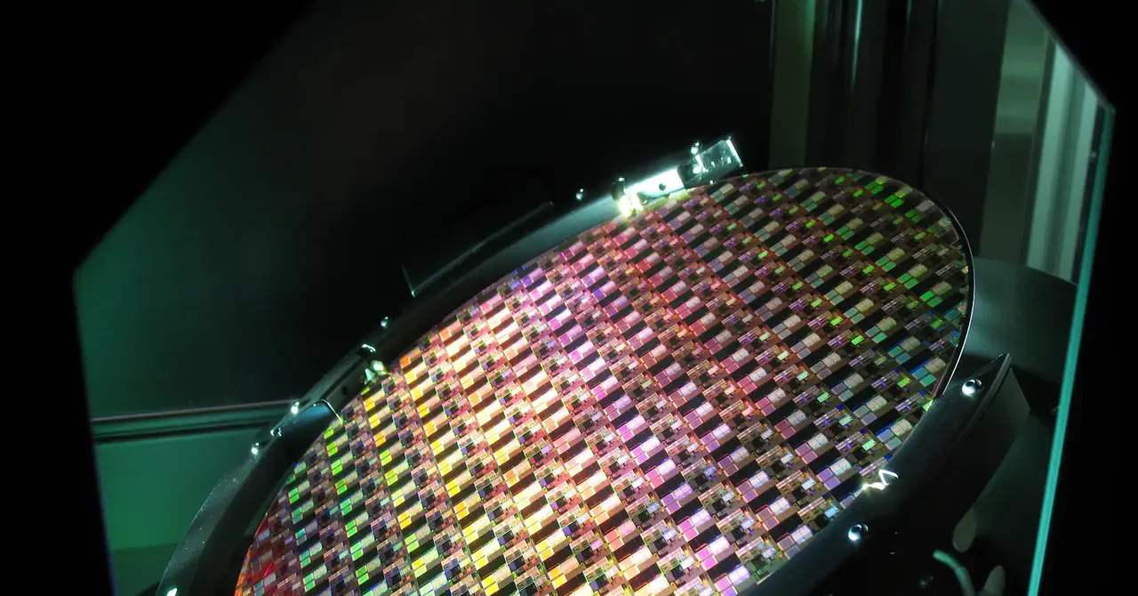
The company says it has tested its technology on around 2,000 wafers so far. That is a meaningful development stage, but still far from the volumes needed for commercial relevance in the global memory market.
Kepler plans to ship its first HBM samples later this year, begin ramping production from Singapore next year and start US production in 2028. Each milestone will test whether the process can hold up under industrial conditions.
GlobalFoundries’ Ed Kaste said the company believes the key breakthroughs are in place, but emphasized that the next step is demonstrating consistency across large numbers of wafers and devices.
Kaste warned that one issue with Kepler’s material system is contamination control, noting that iron can be difficult to introduce into a production line and must be carefully isolated or fully encapsulated.
That warning gets to the heart of the scaling challenge. The more unusual the materials, the more difficult it becomes to fit them into a high-volume semiconductor environment.
Why contamination and tooling are such a big deal
Semiconductor manufacturing is unforgiving. Even tiny contamination problems can ruin yields, and new materials can create compatibility issues with existing tools, packaging methods and production flows.
Kepler says its composite material includes iron, although it has not disclosed the exact makeup. The company says the material set is limited and not typical of mainstream ferroelectric systems, but it would not give specifics.
That secrecy is common in chip startups, especially when intellectual property and manufacturing advantages are at stake. Still, secrecy also makes it harder for outsiders to evaluate whether the process can be integrated broadly or only in specialized, tightly controlled environments.
The company’s reliance on dedicated equipment may help solve contamination risks, but it could also limit how easily the technology spreads across the industry. In practice, the value of any new memory process will depend not only on performance, but on whether it can be used without excessive customization.
How does Kepler compare with other chip upstarts?
Kepler is not the only startup trying to disrupt chip manufacturing. Another well-funded company, Substrate, drew attention last year with a lithography method that uses nanoparticles to create fine features on advanced chips.
That announcement, like Kepler’s, sparked skepticism in parts of the industry. Analysts questioned whether the technology could scale to production volumes while meeting strict cost and reliability requirements.
The comparison is useful because it highlights a recurring truth in semiconductors: a breakthrough in principle is not the same as a breakthrough in manufacturing. A process can be elegant and still fail under the pressure of mass production.
Austin Lyons, a chip analyst at Creative Strategies, said the biggest challenge for any such effort is finding a way around contamination, materials complexity and tooling differences while still keeping costs low enough to matter.
Lyons said the central question is whether the innovation can overcome the limits of contamination, material variation and equipment compatibility in a way that makes large-scale production worthwhile.
What happens next for Kepler?
Kepler’s next year will likely determine whether it remains an intriguing memory startup or becomes a major supplier in the AI hardware stack. The company has laid out a fairly aggressive roadmap, but each phase requires proof.
The immediate milestones are straightforward:
- Deliver first HBM samples later this year.
- Increase production from Singapore in 2027.
- Launch US production in 2028.
Those steps will test not only the design, but the repeatability of the process, the yield rates and the ability to manage new materials safely inside semiconductor production environments.
If the company succeeds, it could help reshape the economics of advanced memory and give chipmakers a new option at a time when AI demand is putting extraordinary strain on supply chains. If it falls short, it will join a long list of chip startups that discovered how difficult it is to turn a clever architecture into a mass-market product.
Why this startup matters beyond one product line
Kepler’s emergence is important because it sits at the intersection of several major trends: AI infrastructure spending, memory scarcity, US industrial policy and the race to reduce dependence on costly advanced lithography.
The startup is not claiming to solve every semiconductor problem. Instead, it is targeting one of the most painful constraints in the current market: the ability to move and store data quickly enough to keep AI systems fed.
If memory remains the fuel for the AI era, then whoever can produce it more cheaply, more efficiently and at greater scale will have significant leverage. That is what makes Kepler’s claim worth watching.
The company is still early, and the hardest work remains ahead. But in a market where memory is increasingly strategic, even the promise of a new manufacturing path can attract major capital, government attention and industry interest.
| Milestone | Expected timing | Potential significance |
|---|---|---|
| First HBM samples | Later this year | Initial proof that the architecture can be packaged into usable product |
| Singapore production ramp | Next year | First step toward higher-volume manufacturing |
| US production | 2028 | Key for domestic supply chain goals and scale-up |
| Wafers tested so far | About 2,000 | Shows progress, but still far from commercial volumes |
For now, Kepler’s story is less about a finished product than about a challenge to one of the semiconductor industry’s most expensive assumptions: that the only way forward is to keep building bigger, costlier fabs and keep leaning on EUV. The startup is betting there is another route.
Whether that route leads to mass production will depend on the next set of tests, and on whether the chip industry is ready to embrace a memory platform that tries to grow by redesigning the physics, not just the fab.
Frequently asked questions
What is Kepler Computing trying to do?
Kepler Computing is trying to redesign high-bandwidth memory and SRAM so chips can store and move data more efficiently without relying on the most expensive advanced lithography tools. The startup says its approach could help relieve the AI memory shortage if it scales successfully.
How much funding has Kepler raised?
Kepler has raised $468 million from investors including GlobalFoundries, Intel Capital, AMD Ventures, Baillie Gifford and Bill Gates’ Gates Frontier fund. The US Commerce Department has also committed up to $245 million in support.
Why is Kepler’s technology different from conventional chipmaking?
Kepler says its memory architecture uses 3D stacking and new materials to increase density rather than depending on extreme ultraviolet lithography. That could let it use existing fabs more effectively and avoid some of the cost and complexity of building new ones.
When will Kepler’s chips be available?
Kepler says it plans to ship its first HBM samples later this year, ramp production out of Singapore next year and begin US production in 2028. Those dates remain contingent on successful scaling and manufacturing validation.
What is the biggest risk for Kepler?
The biggest risk is scale. Kepler has tested on roughly 2,000 wafers, but moving from lab-scale or pilot production to millions of devices is difficult, especially when new materials can create contamination and tooling challenges.